What does PCB Circuit Board Exposure do?
2020-08-04

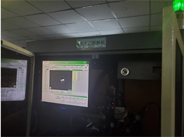
As a Finishing PCB Technologies Supplier, share with you. PCB circuit board exposure has two types: circuit exposure and solder mask exposure. The function is to cure the irradiated local area through ultraviolet light irradiation, and then develop it to form a circuit pattern or solder resist pattern.
The process of line exposure is to first attach a photosensitive film to the copper clad board, and then put it together with the circuit pattern negative and expose it with ultraviolet rays. The photosensitive film irradiated by ultraviolet rays will undergo polymerization reaction. The photosensitive film here can resist Na2CO3 weak alkali during development. The solution is washed away, and the unexposed parts will be washed away during development. In this way, the circuit pattern on the negative film is successfully transferred to the copper clad board;
The process of solder mask exposure is the same: apply photosensitive paint on the circuit board, and then cover the areas that need to be soldered during exposure, so that the pads are exposed after development.
Making a PCB board is not a simple process to finish the board, just drill a hole and punch the components. The production of PCB board is not difficult, but the difficulty lies in troubleshooting after the production is completed. Whether it is a personal hobbyist or an industrial engineer, it is quite a headache for the PCB circuit board to encounter problems when debugging, just like a programmer encounters a BUG.
Some people have a strong interest in debugging PCB circuit boards. Just like programmers solving BUG, there are not many common PCB circuit board problems. Common problems are except for circuit board design, damage to electronic components, short circuits, and components. The quality of the PCB circuit board disconnection faults are not rare.
Common PCB circuit board failures are mainly concentrated on the components, such as capacitors, resistors, inductors, diodes, triodes, field effect tubes, etc. The integrated chips and crystal oscillators are obviously damaged, and the more intuitive way to judge the failure of these components can be through Eyes to observe. Obviously damaged electronic components have obvious burn marks on the surface. Such failures can be solved by directly replacing the problematic components with new ones.
Of course, not all electronic component damage can be observed with the naked eye, such as the resistors, capacitors, diodes, etc. mentioned above. In some cases, the damage cannot be seen from the surface, and it needs to be repaired with professional inspection tools. Commonly used inspections include: multimeters, capacitance meters, etc., when the voltage or current of a certain electronic component is detected to be out of the normal range, it indicates that there is a problem with the component or the previous component, directly replace it and check to see if it is normal.
Our company also has Aluminum PCB on sale, welcome to contact us.
